An Introduction to
Micromechanical Actuators
A Device Overview and a Specific Application

Introduction to the Micro Actuator Project
Note: There are many interesting images
on this page. It may take a few minutes for the page to fully load.
The curriculum for Elec
435, Electro Mechanical Devices, an Electrical
Engineering course at Rice University
,
requires that class members undertake a project to examine an actuator
or sensor which was not covered in classroom lecture. Material gathered
is to be presented in a formal report or on a project web page (this document).
In addition, there is an in class oral presentation.
I have selected the subject of micro actuators. Within this broad
scope I will present material on the following topics:
Introduction to Micro Actuators
A Brief Look at Lithography and Micro Machining
An Overview of Micro Actuator Types
The DMD - An Application of an Electrostatic Actuator
References
This course was taught in the Fall, 1996 semester by Professor J.
D. Wise .
This project web page was prepared by Wayne
Herbert who is solely repsonsible for its content. Email
me with your comments and questions. If you feel that I have
used any proprietary material, or have not given sufficient credit for
material obtained from the web, please contact me and I will rectify the
situation.
Introduction To Micro Actuators
One result of the increasing technical sophistication of humankind has
been the shrinking of the devices which power our world. Modern internal
combustion engines put out far more horsepower per unit of weight and displacement
than did their predecessors. Modern electric motors take advantage of high
strength magnets and sophisticated windings to produce lots of power in
a small package.
Until recently though, any power producing device could be seen by
the naked eye. Although some attempts were made to create minature motors,
efforts were limited by the lack of tools needed to build on such a small
scale, and a lack of understanding of the physical forces which occur at
this scale.
The revolution in electronics miniaturization, perhaps more than
anything, has provided a strong impetus in the drive towards ever smaller
power devices. Vacuum tubes have been replaced by transistors which can
be created by the tens of thousands on small silicon based chips. It is
this miniaturization, and the attendant advances in micro
machining and lithography
necessary
to create such electronics, that have fostered the growth of micro actuator
research and development. Research in this area has been particularly active
in Japan, where a consortium of businesses and universities has pooled
their resources to maximize the benefits of research.
It should be noted that while the field of microsensors is broad
and constantly expanding into new commercial applications, micro actuators
have found use in only a few narrow applications, because of the difficulty
of designing and building devices that can deliver sufficient power and
displacement to make them worthy of connection to real world mechanical
loads.
A Brief Look at Lithography and Micro Machining
One of the most important aspects of micro scale manufacturing is lithography,
a photographic process by which the details of an electronic circuit, or
the parts for a micro actuator, are etched into some base, usually silicon.
Although far more detailed and complex, the process basically works as
follows:
-
a silicon wafer is coated with a photographically sensitive material.
A mask containing all or some of the desired elements in the final product
is laid over the silicon wafer, and it is exposed with light.
-
through chemical processing only the exposed material is left on the
silicon wafer (similar to developing film from a camera). These areas may
be etched to create holes, wells, or other structures, or they may have
additional material laid upon them (such as an electrically conductive
material).
-
the process is repeated for each layer to be produced on the chip until
the complete circuit or device is present. Electrical connections are added
to the circuit, and it is wrapped in a suitable package to protect it.
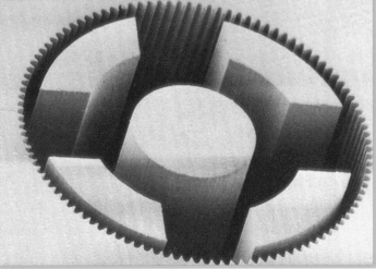
A major advance in the construction of micro actuators is a lithographic
technique called deep
x-ray lithography (DXRL) , a process which allows much deeper etching
in silicon, and hence more robust micro devices such as the mold for a
micro gear shown below. This gear is 400 micrometers in diameter. Continued
advances in lithography, such as x-ray lihtography, atom lithography, and
electron lithography, are making micro construction all the more practical.
Micro
machining is accomplished through the use of equipment such as lasers,
scanning electron microscopes, and scanning tunneling microscopes. IBM
has successfully created their logo using a scanning tunneling microscope
to move individual atoms to their correct location. Bell Labs is using
finely focused, low power laser beams as tweezers to grab cells and other
organic material.
Overview of Actuator Types
As might be expected, virtually every type of force generating mechanism
conceived has been implemented in the world of microactuators. Force generating
mechanisms fall into the categories of electromagnetics, capacitive (electrostatic)
devices, piezoelectrics and ultrasonic devices, and fluid driven devices.
As noted above, virtually all of these devices are created in silicon using
lithographic techniques.
Electromagnetic Devices
Piezoelectric Devices
Ultrasonic Devices
Electrostatic Devices
Fluid Devices
Electromagnetic Devices
In the area of electromagnetic devices, several companies have produced
conventional electric motors at a micro scale. For example, Yasakawa Motors
has created an electric motor which uses .2 mm wires and thin film magnets
to drive a 2.5 mm diameter two phase rotor. Nippondenso Corporation has
created a 1.0 mm motor using a permanent magnet rotor which develops a
micro newton-meter of torque when supplied with 3 V at 20 mA. Several companies
have also produced linear stepper motors which are designed to insert micro
miniature catheters into a variety of materials, including cells.
One of the primary advantages of electromagnetic devices is their
high power output compared to electrostatic devices. However, electromagnetic
motors suffer from several problems. The largest of these problems is fabrication.
Almost all fabrication is done using a silicon substrate and using lithographic
techniques borrowed from integrated circuit manufacturing. It turns out
to be very difficult to create electromagnetic coils and permanent magnets
in silicon using current technology. Instead, such items must be "glued"
to the package once assembly is complete, thereby limiting placement and
increasing costs. However advances in electromagnetic motors are being
made as evidenced from the two motors shown below, courtesy of the University
of Sheffield , United Kingdom. Both are three phase inductor motors;
the one on the right uses an aluminum rotor.
Piezoelectric Devices
A booming area in micro actuators are the piezoelectric devices. These
devices use an interesting phenomenon found in some crystals, namely, that
a force upon the crystal (a distortion) produces a voltage, and when a
voltage potential is placed across the crystal, it distorts, creating a
force. The earliest work in piezoelectrics was done by Pierre and Jacques
Curie in the 1880's using tourmaline, quartz, and cane sugar cyrstals.
Modern piezoelectric devices are ceramic composites and feature a
very high range of motion for a given electrical input when compared to
early crystal forms. In addition, the ability to lay these ceramics as
thin films onto silicon substrates, through sputtering and other processes,
has enabled these devices to be readily integrated into the world of electronic
integrated circuits.
Advantages of ceramic piezoelectric devices include very high resolution,
zero "sticking" friction, fast response, no wear, high stiffness, and relatively
low voltage (100 V) operation. Disadvantages include a very short range
of operation, mostly linear motion, and fairly high cost. Rotating devices
can be constructed which use bending elements constructed in a rotor. The
elements bend when a voltage is applied, and catch in cavities in the wall
surrounding the rotor, causing the rotor to turn (see also Ultrasonic Devices,
below).
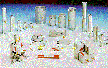
Piezoelectric actuators are amongst the most developed of all micro
actuators and several companies have taken them out of the lab and into
the commercial world. Examples of packaged actuators (no, the package is
not micro miniature!) are shown below.
For more information concerning ongoing piezoelectric motor research,
try the University of Missouri-Rolla
.
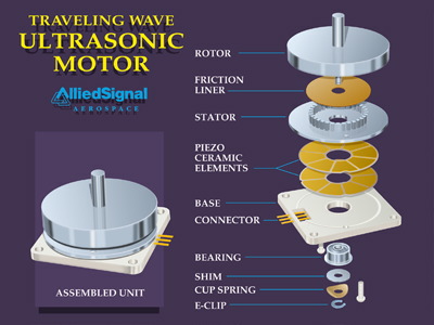
Ultrasonic Devices
A most useful application of piezoelectric devices is in the construction
of ultrasonic motors. A piezoelectric device operates at a very high (ultrasonic)
frequency while sandwiched between the rotor, stator, and a friction liner.
Each pulse of the piezoelectric device causes it to expand against the
friction liner, driving the rotor.
Adavantages of the ultrasonic motor include high power in a low volume
(higher even than an electromagnetic motor), and high torque at very low
speeds. The primary disadvantage of these devices is the relatively low
operating life because of the wear between the resonator and the rotor.
Thus, these motors will be found in intermittent use applications such
as the motor which drives the focusing ring in autofocus cameras.
An example of an ultrasonic motor is shown below. Again, try the
University
of Missouri-Rolla for lots of useful information concerning ultrasonic
motors.
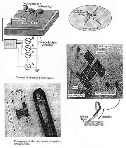
An "odd" type of ultrasound related actuator is the vibration driven
device. The actuator works by being coupled to the outside world at some
resonant frequency, wherein the vibration creates motion within the device.
An interesting application of this technology is a mechanical
ant whose limbs are connected to such devices, and which will walk
when placed upon a vibrating platform. A picture of this device is shown
below.
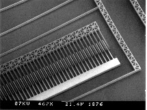
Electrostatic Devices
All electrostatic devices operate on the principle that opposite charges
attract. There are multiple ways in which this phenomenon is implemented
in micro actuators.
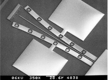
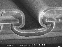
One such implementation is the cantilever beam. A bendable beam,
which is also one of the electrodes is placed between two more electrodes.
Upon application of suitable voltage, the cantilever device bends. This
devices offer motion in the range of 10's of micrometers, and forces ranging
into the 10's of mN. An example of such a beam is shown below.
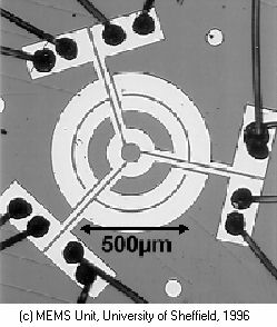
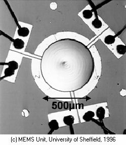
Yet another type of electrostatic motor is the wobble motor. Stator
poles are placed around a disc (rotor) which is at an angle with respect
to the plane of the stator poles. As a voltage is applied to each stator,
the disc is attracted to that stator and "wobbles". Connected to the disc
is an inner ring which provided continuous rotational motion derived from
the wobble. Such motors offer 10's of RPM and fairly strong torque characteristics.
In addition, they are readily fabricated on a silicon substrate.
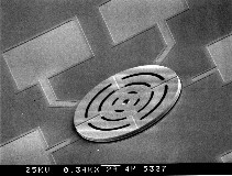
A four stator wobble motor (500 microns) and its bearing support
(right)
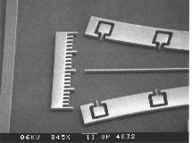
Still another type of electrostatic actuator is the comb drive. Two
sets of interlinking "fingers" attract or repel one another creating linear
motion. An example of a comb drive is shown in the pictures below.
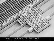
All photos courtesy of University
of Twente
Fluid Driven Devices
In addition to the more "mainstream" types of actuators described above,
two other actuator types are worthy of mention. The first is a micro scale
steam engine. This device was originally developed at Sandia Laboratories.
It is constructed with a piston driven by a steam source. Its big advantage
over other device types is the large amount of force that it can generate,
about 1.16 uN, or about 100 times the force generated by a typical electrostatic
device. On the down side, it is a very slow machine. It takes approximately
.1 second for the thrust cycle, and 1 second for the piston to return to
the beginning of its stroke. In addition, the water evaporates over time,
so it eventually loses its driving fluid.
The second "odd" actuator type is a fluid driven gear system, essentially
a tiny version of a turbine or water wheel. Pathways for water or other
fluid are etched into a silicon chip, along with the "vessel" which holds
the rotating water wheel. The bearing for the wheel is also etched into
the silicon. A small gear like wheel acts as the turbine. Once inserted,
a covering piece of silicon is added, with access to the wheel's shaft.
An advantage of this device is a complete lack of electric or magnetic
fields, making it suitable for use in volatile environments, or where electromagnetic
contamination might affect sensitive measurements. A disadvantage is the
complex support equipment consisting of pumps, hoses, and valves.
The DMD - An Application of an Electrostatic Actuator
Introduction
Construction and Mechanical Operation
Operation as a Video Device
Introduction
One of the more fascinating applications of electrostatic actuators
is the "Digital Micromirror Device", or "DMD". Developed by Larry J. Hornbeck
of Texas Instruments, Digital Light Processing,
this device combines aluminum alloy mirrors, silicon based electrostatic
drives, and silicon micro electronics to create a "light switch". Because
the entire device is micro machined on a single silicon chip, each mirror
is so small that "dozens of them are covered by the tip of a standard
straight pin". It is expected that these mirror devices will play a major
role in the next generation of video displays and hard copy printers. An
example of the device is shown below.
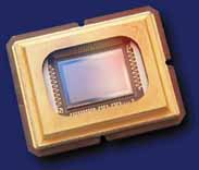
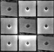
This is an 848 x 600 Digital Micromirror Device. The central, reflective
portion of the device consists of 508,800 tiny, tiltable mirrors. A glass
window seals and protects the mirrors. Each mirror is 16 um on a side.
Construction and Mechanical Operation
Construction
Operation
The incredible degree of miniaturization found in micro electronics
seems all the more awesome when combined with mechanical devices. The two
together are called "Micro Electro Mechanical Systems" or "MEMS". The DMD
is a "monolithically integrated" MEMS cell, which means that the entire
structure which is about to be described is created in a single lithographic/micromachining
process. Certainly, the process itself is very complex, but the important
fact is that this mechanical device can be created just as an integrated
circuit would be built. The alternative process, for example, that which
might be used to create an electromagnetic micromotor, requires that silicon
processing be followed by another process such as gluing a permanent magnet
to a sillicon base.
Construction
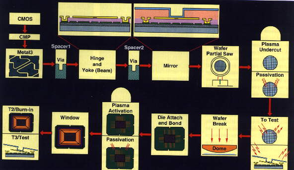
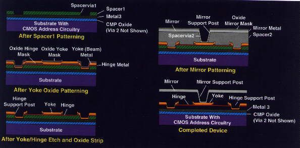
Using a modified lithographic process, the device shown below is created
as follows:
-
the memory cell and associated electronics are laid down on the silicon
substrate. These steps closely follow current integrated circuit production
techniques.
-
using a specially layered overlay, the electromechanical parts of the
cell are created. This includes the electrical contacts (mirror electrodes,
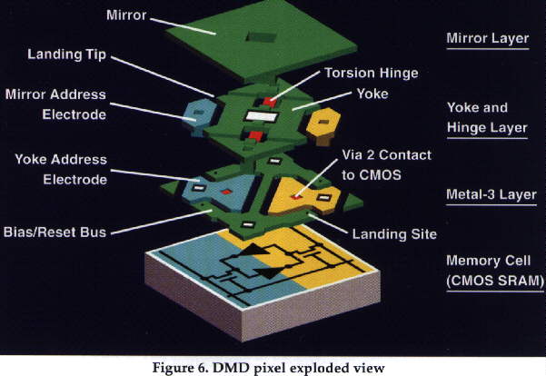
yokes electrodes), and the mechanical parts (the torsion hinge, mirror
support post, electrode supports).
-
aluminum alloy is overlaid on the mirrors. Then, through a deep etching
process, the material between the base electronics circuits and the mirrors
is removed to provide the air gap necessary to allow the mirror to tilt.
Interestingly enough, the entire manufacturing process closely follows
standard techniques for semiconductor manfacture. Lithography, sputter
metal deposition, and plasma etching are all used in the DMD process. Even
the sacrificial layer is a standard hardened positive photoresist layer.
However, there are steps in the process which are different (and undisclosed,
apparently due to the proprietary nature of the process).
The first figure below outlines the general processing flow for a
DMD chip, while the second provides a more detailed view of the manner
in which the DMD portion of the chip is actually constructed.
Operation
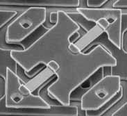
The mirror is connected to the yoke which can rotate on the two torsion
hinges which run through it. Under the yoke itself are the yoke address
electrodes. The yoke is attracted to one or the other of the yoke address
electrodes depending upon which is energized. Which of the electrodes is
energized depends, in turn, upon the status of the memory cell directly
beneath it. A "one" stored in the cell causes the mirror to move to a +
10 degree position (at which point it contacts the yoke and becomes mechanically
connected via the landing site contacts). When the memory cell contains
a zero, the mirror moves to a - 10 degree position. When the memory cell
is neither, no electrostatic force is applied to the mirror and the torsion
hinges cause the mirror to return to 0 degrees.
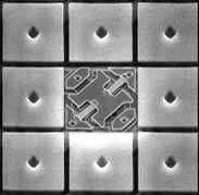
When a mirror is fully tilted in either direction, and has made contact
with the yoke base, a bias current keeps the mirror in place irrespective
of changes in the address electrode. This enables the mirror to remain
in the correct position even while a new bit of data is being loaded into
the cell memory. An example of the positive deflection position, as well
as an actual picture of the mechanism underlying the mirror (the yoke and
torsion hinges are readily observable), is shown below.
Operation as a Video Device
The DLP chip can be utilized in three different ways to project an image.
All are discussed in some depth at the TI
Digital Light Processing Web Site . Of the three methods, the simplest
implementation uses a single DLP chip.
The mechanical construction and layout of the projection device is
shown below. A white light source is projected first through a rotating
color wheel, through a focusing lens, and then onto the DLP chip. Light
from the chip, when the mirrors are correctly positioned, is reflected
to the projection lens, and from there to the display panel.
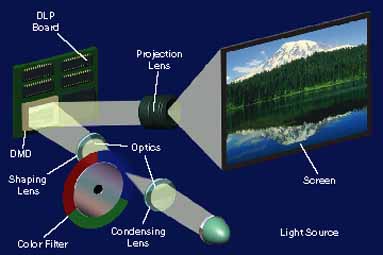
A one-chip DLP projection system. White light is focused down onto
a color wheel filter system that spins at 60 Hz. This wheel spins in sequence
with the red, green, and blue video signal being sent to the DMD. Mirrors
are turned on, depending on where and how much of each color is needed
for each TV field. The human visual system integrates the sequential color
and sees a full-color image.
Details of the video display operations follow.
-
The color wheel rotates at 60 rotations per second. This means that
there are 180 color changes per second as a result of the turning wheel.
-
This means that each color passes through the light source for approximately
5.56 ms for each revolution of the wheel.
-
Thus, if the color for a particular pixel is to be switched on, the
mirror must be capable of moving to its correct position in less than 5.56
ms. In reality, the mirror can be move from one maximum deflection to the
other in a period of less than 20 microseconds.
-
This means that for any given color, the mirror for any pixel can move
a total of 5.56 ms / 20 us = 278 times while the color is moving past the
light source. Or to put it another way, the length of time that a mirror
can be turned towards the projection lens can vary from 1 part in 278 to
278 parts in 278.
-
Rather than use 278, one byte of 8 bits is used to control the mirror
movement. 8 bits yields 256 possible timings for the mirror.
The cycle for one frame of display proceeds as follows.
-
The video signal is received by the chip and is separated into its red,
green, and blue components.
-
For each color component (let's work with red), its intensity is translated
to a value between 0 and 255 and stored in the mirror control byte.
-
Using the reset/latch bias currents, all mirrors in the array are returned
to their neutral position. Then the most significant bit is sent to the
mirror memory cell and the latch current is turned on. If the bit was a
'one' the mirror deflects towards the projection lens and is latched; if
'zero' the mirror deflects to - 10 degrees and no light is sent to the
lens.
-
While the mirrors are latched in place, the next bit in the intensity
byte is sent to each mirror's memory cell. Once in the cell, the reset/latch
bias currents return the mirror to the neutral position and then either
to + 10 degrees or - 10 degrees, depending once again upon the contents
of the memory cell.
-
This process continues until all the bits in the intensity byte have
been transmitted to the memory cell and the mirror moved in response. It
should be noted that the total time that a mirror is "on" depends on which
bit is being processed; the most significant bit stays "on" the longest
while the least sifnigicant bit is the shortest.
-
Thus, to process a single frame of video each mirror will move 8 times;
for maximum intensity, all 8 times will result in a positive deflection,
while minimum intensity results in 8 negative deflections. Intermediate
intensities require that the mirror move in both directions at a ration
equal to the desired intensity.
-
The net effect is that for each pixel, anywhere from 0 to 255 flashes
of a specific color will be reflected to the projection lens. Because the
cycle time is so much faster than the integration time of the human brain
and eye, the multiple flashes are perceived as intensity
It should be noted that with the single mirror chip system, only one
third of the total light intensity is actually transmitted to the projection
lens since the other two primary colors are always filtered out. This problem
is readily overcome by the use of three DLP chips which are run together
synchronously. The light from the white source is prismatically split into
the three primary colors and forwarded to each DLP chip. A further advantage
of this method is the ability to use even higher color resolution than
that available with a single chip. Since any given mirror need deal with
only one color during a given cycle, the total amount of time, and hence
the total number of times the mirror may switch is increased my a factor
of three.
Applications and Reliability
Given that a chip which will support super VGA resolution (800 x 600)
will contain nearly a million hinges, hinge fatigue could be a serious
problem. However, the device has been tested by subjecting each mirror
to more than 1 trillion cycles in an accelerated period. This is equivalent
to about 20 years worth of normal use without failure. Other problems,
including the sticking of the mirror to its landing site (stiction), and
the permanent bending of the hinges so that the mirror no longer returns
to a flat position have been overcome with the selection of suitable materials.
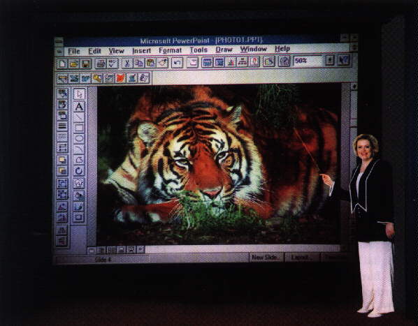
Initial applications will include a business projector and a board
with the chip which can be integrated into a complete video system. TI
has created a very large display (shown below) to demonstrate the brightness
and effectiveness of the DLP chip and DMD technology.
References
Material Available on the Web and Used in This Document
Micro
Scale Steam Engines
Operation of Piezoelectric
Devices
Electromagnetic
Micro Motors
Additional Related Material Available on the Web
Atom
Lithography
A
Large List of Links to Related Web Sites
Electrostatically
Driven Mirrors in Laser Scanners
Books, Papers, and Journals
"Basic Electrical Power and Machines", David Bradley, Chapman and
Hall
"Micromechanical Sensors, Actuators, and Systems, D. Cho, et al,
A.S.M.E.
This page was last modified on December 13, 1996, AD. God bless the
Queen. If you have kudos and accolades for this page, contact Wayne
Herbert, but if you want to gripe, try Art
Farkel.

Copyright © 1996 Wayne Herbert
Go to Wayne Herbert's
Home Page